Bandwidth Gap
An emerging issue in the computing industry over the last several years is the bandwidth gap between the major communication interfaces (PCIe, Ethernet, USB, etc.), and the external memory interfaces (typically DDR3/4).
Ethernet has increased from 10 Gbps, to 40 Gbps, then 100 Gbps, and recently to 400 Gbps. Similarly PCIe has increased from 2.5 GT/s per lane, up to 16 lanes (Gen1), to 5.0 GT/s (Gen2), to 8.0 GT/s (Gen3), to 16.0 GT/s (Gen4). PCIe Gen5 is expected to be released in 2019 with a bandwidth of 32 GT/s per lane. Gen 5 x16 will provide a bandwidth of 512 GT/s in each direction. USB has also increased from 5 Gbps (USB3.0), to 10 Gbps (USB3.1), to 20 Gbps (USB3.2). USB4 is expected to be released in 2019 with a bandwidth of 40 Gbps.
In comparison, the DDR bandwidths have only increased from 1066 MT/s per pin (DDR2) to 2133 MT/s (DDR3) to 3200 MT/S (DDR4). Most FPGAs only support the lower 2400 MT/s or 2667 MT/s variants of DDR4. DDR5 is expected to be released in 2019. Memory manufacturers are reporting bandwidths of 6400 MT/s and 7500 MT/s. DDR5 will help to reduce the bandwidth gap. However, other memory technologies have emerged to address the bandwidth gap issue.
HMC
Hybrid memory cube (HMC), is a 3D stacked die DRAM memory solution that uses high-speed serial interfaces to connect with 1 to 4 external memory masters. HMC1.0 devices featured x8 or x16 lane configurations, running at 10, 12.5 or 15 GT/s. The HMC2.0 specification increased the line rates up to 30 Gbps; however, the actual DRAM memory bandwidth is limited to less than the line rate bandwidth due to internal memory interfacing limitations. In fall 2018, Micron announced the discontinuation of their HMC memory devices.
HBM
In the last few years, the memory industry has been focusing on the High Bandwidth Memory (HBM) devices. HBM is also a 3D stacked die DRAM memory solution. The high bandwidth is obtained via a very width data bus (typically 1024-bits). HBM is coupled with GPU, CPU, or FPGA devices by mounting both devices on a silicon interposer which provides the large number of interconnects required by the HBM interface. Pairing the HBM core with the memory host device eliminates resources for external memory interfaces, Printed Circuit Board (PCB) routing, and PCB board space. HBM1 supports 4 or 8 high DRAM die stack arranged in 8 channels of 128 bits each (1024-bits total) at a line rate of 1 GT/s per data bit. This provides a bandwidth of 128 GBps. Typical DRAM densities are 2 GB per die, so an 8 high stack provides 16 GB of storage.
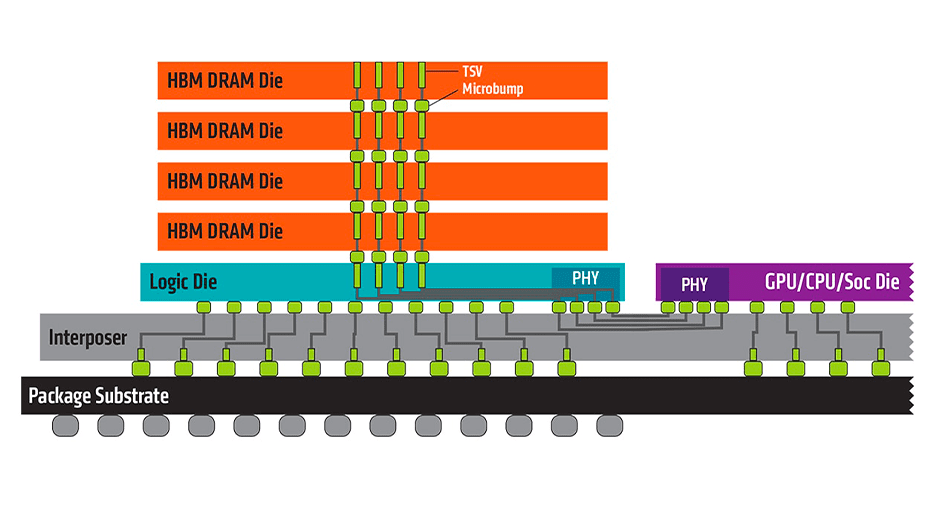
Figure 1: High Bandwidth Memory and Interposer (https://www.amd.com/system/files/49010-high-bandwidth-memory-hbm-1260×709.jpg)
The HBM2 specification increased the line rate to 2 GT/s, thus doubling the bandwidth to 256 GBps. In 2018, JEDEC further increased the specification to support a line rate of 2.4 GT/s (307 GBps bandwidth) and increased the memory stack height to 12 DRAMs (24 GB storage).
HBM3, expected in 2019 or 2020, is anticipated to have a bandwidth of 512 GBps or higher and larger storage capacity by increase die density, stack height, and line rate.
HBM and FPGAs
Both Xilinx (Virtex Ultrascale+) and Intel (Stratix 10 MX) have added High Bandwidth Memory to their FPGA devices. While, there are similarities in their product offerings, there are also important differences in performance, interfacing, and bandwidth limitations. The table below compares the HBM features between these FPGA devices.
Feature
Xilinx (Virtex Ultrascale+)
Intel (Stratix 10 MX)
Number of HBM Stacks
2
2
Total Storage (GB)
4, 8
8, 16
Channels (per HBM Stack)
8
8
Pseudo Channels (per HBM Stack)
16
16
Data Width per Pseudo Channel
64
64
Total Data Width per HBM Stack (bits)
1024
1024
Memory Clock Frequency (MHz)
900
1000
Bandwidth per HBM Stack (GBps)
230
256
Stack Configuration
Left, Right, Both
Top, Bottom
FPGA Interfaces
16 AXI3 Ports (256-bit)
16 AXI4 Ports (256-bit)
AXI Interface Clock Rate (MHz)
450
Depends on speed grade
Hard AXI Switch Fabric
Yes
No
Soft AXI Switch Fabric
Not needed
Required to access full address range
Table 1: Comparison of HBM features in Xilinx and Intel FPGA Devices The Intel Stratix 10 MX device has two times the HBM memory storage of the Xilinx Virtex Ultrascale+. The Intel device also has slightly higher bandwidth than the Xilinx device.
AXI Switch Fabric
The memory arrangement is the same for both FPGA vendors. The HBM memory is divided into 8 channels, each with two pseudo channels. Each pseudo channel is mapped to a separate AXI port. In order to access HBM memory in a different pseudo channel, AXI switch fabric is required. Xilinx has opted to provide hard AXI switch fabric to enable access to the full HBM address space from any AXI port. On the other hand, the Intel device requires addition of soft AXI switch fabric to provide HBM address space access across pseudo channels.
For both FPGA devices, each AXI port only has access to 1/16th of the total HBM bandwidth. In the Xilinx device, the hard AXI switch fabric is divided into 4 sub-switches with each sub-switch supporting 4 adjacent AXI ports. There are only 2 AXI interconnect between the sub-switches. If all 4 AXI ports on the sub-switch are accessing pseudo channels in the adjacent sub-switch, then the AXI bandwidth is reduced by half, due to the switch arbitration of the 4 AXI ports, through the 2 adjacent sub-switch AXI interconnect paths. In the case of AXI write accesses, there is one clock cycle of dead-time in order to switch between AXI sources. In the case of small burst sizes, this can result in only 25% of the available bandwidth. For the Intel device, the bandwidth limitations through the AXI switch fabric are dependent on the user instantiated AXI interconnect. It may also have similar limitations. These bandwidth limitations must be kept in mind when designing the FPGA interfacing to the HBM.
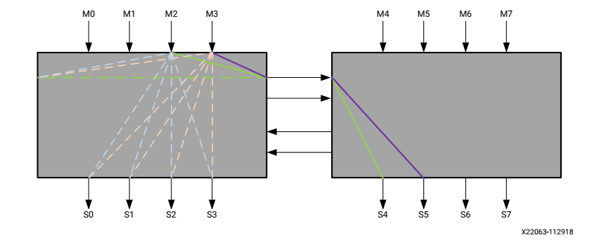
Figure 2: Xilinx Ultrascale+ HBM AXI Switch Fabric Interconnect (PG276, Figure 3)
The Xilinx Ultrascale+ HBM provides the option to instantiate both stacks together to double the storage capacity and bandwidth, and uses double the number of AXI ports (32). For the Intel Stratix 10 MX, the HBM stacks are on opposite sides of the FPGA die. Each HBM memory stack must be instantiated separately and the AXI interconnect between HBM memory stacks must cross the entire FPGA die. This will require extra pipelining (increased latency) or will have reduced performances (lower bandwidth due to lower AXI clock frequency). However, the HBM stacks in the Intel device have twice the capacity of the Xilinx device, and most applications do not require the bandwidth of a two stack system. For applications that require using both HBM stacks, the design needs to take into account the physical architecture of the HBM structures in the target FPGA device.
Due to the AXI interfacing and switch fabric, the HBM is most suited to applications that can work with 16 independent memory storage spaces, with no accesses between HBM pseudo channels. This configuration will maximize HBM bandwidth. Since this is not the case for most applications, alternative interfacing strategies must be considered.
Conclusions
High Bandwidth Memory provides a pathway to address the bandwidth gap between computing interfaces and memory storage. Both Xilinx and Intel FPGAs have HBM storage. The AXI interconnect fabric places limitations on the HBM bandwidth available. Careful design of the user logic and HBM interfacing is necessary in order to meet the user application storage and bandwidth requirements.
If you think High Bandwidth Memory may be a fit for your application, contact Nuvation Engineering to learn about how we can provide FPGA, hardware, and embedded software design services to move your product from conception through to manufacturing.