
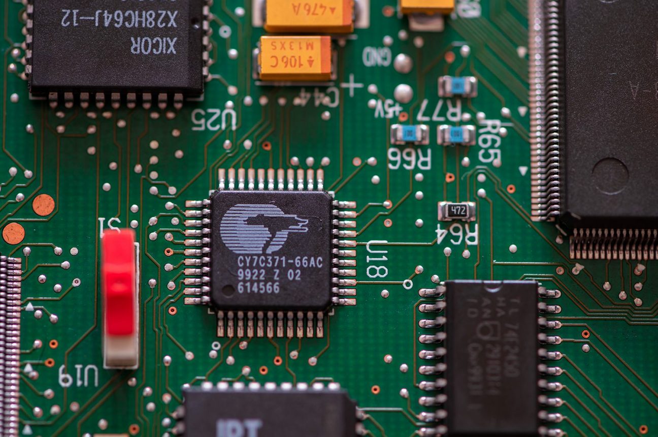
Addressing SI & EMC Challenges in High-Speed PCB Design
As digital systems move into higher speeds and tighter form factors, design teams often encounter performance issues they may not anticipate. Many of those issues stem from signal integrity (SI) and electromagnetic compatibility[…]
Nuvation Engineering - December 9, 2025
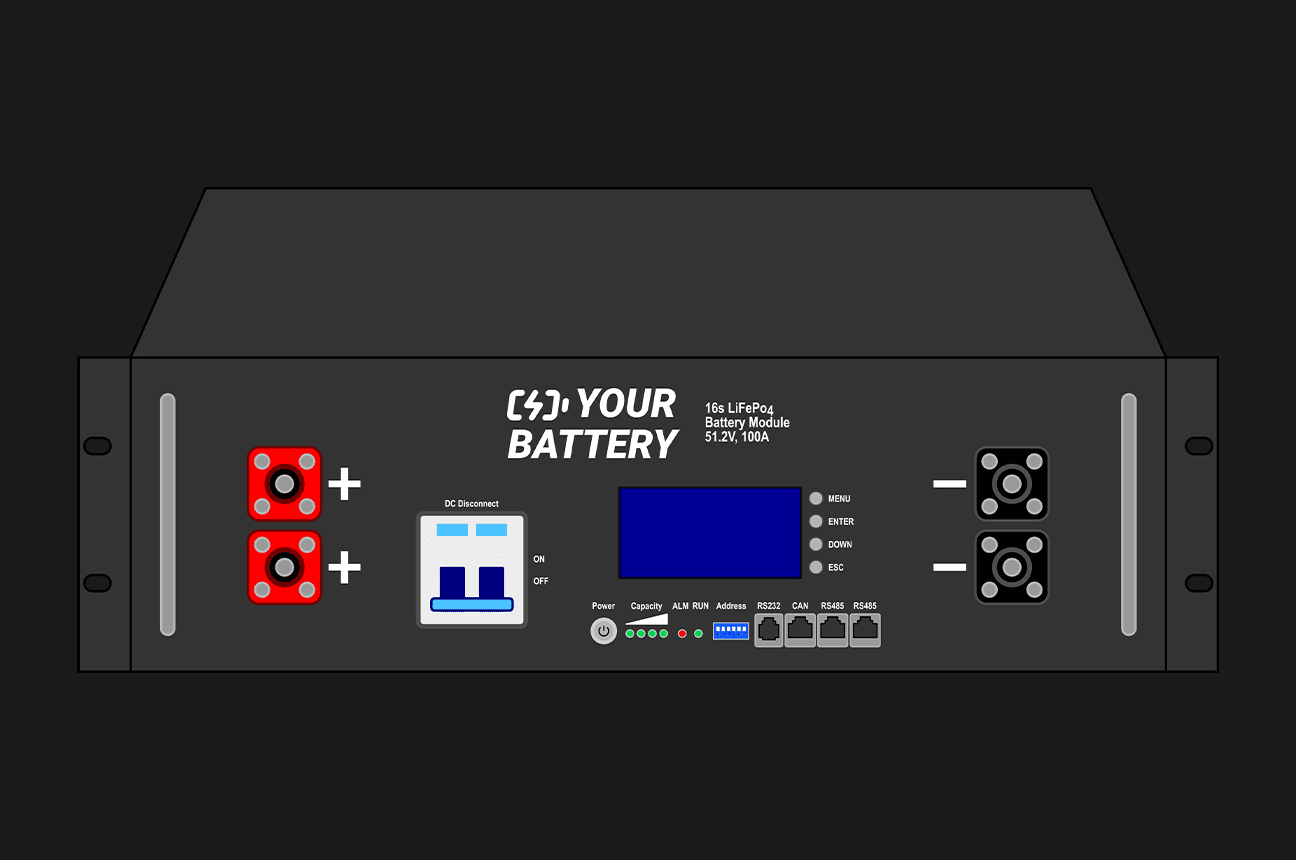
Defining Your Custom BMS Requirements
A strong energy storage system starts with the right battery management system. Learn how defining clear requirements early can shape performance, safety, and long-term reliability. Selecting the right Battery Management System (BMS) is[…]
Nuvation Engineering - October 28, 2025

FPGAs for Fiber Networks in Industrial Applications
Communication networks are essential in industrial applications for gathering sensor inputs, distributing actuator outputs and for system configuration, control, and health monitoring. It is important to select the network type based on bandwidth[…]
Nuvation Engineering - September 15, 2025

Nuvation Selected for Purigen Biosystems’ Revolutionary DNA Extraction Instrument
Nuvation Engineering provided custom board design, firmware development, and regulatory compliance testing support for Purigen’s revolutionary DNA extraction and purification device. June 12, 2020, Sunnyvale, CA. Purigen Biosystems selected Nuvation Engineering to provide hardware and[…]
Nuvation Engineering - July 3, 2024

Hardware Bee Interviews Nuvation CEO Michael Worry
Discover the Latest Innovations and Opportunities Shaping the Future of Digital Finance. Stay ahead of the curve with insights into emerging technologies, investment strategies, and market developments in the dynamic world of cryptocurrency.
Nuvation Engineering - April 26, 2024

Important Design Considerations for Electronic Devices: Part 4 – Data Security
Over the past two decades Nuvation Engineering has developed electronic devices for a wide range of market applications. Based on our experience across hundreds of engineering design projects, our engineers have identified several[…]
Nuvation Engineering - March 13, 2024
Addressing SI & EMC Challenges in High-Speed PCB Design
As digital systems move into higher speeds and tighter form factors, design teams often encounter performance[…]
Nuvation Engineering - December 9, 2025
Defining Your Custom BMS Requirements
A strong energy storage system starts with the right battery management system. Learn how defining clear[…]
Nuvation Engineering - October 28, 2025
FPGAs for Fiber Networks in Industrial Applications
Communication networks are essential in industrial applications for gathering sensor inputs, distributing actuator outputs and for[…]
Nuvation Engineering - September 15, 2025
Important Electronic Design Considerations for Electronic Devices: Part 1 – Calibration
Over the past two decades Nuvation Engineering has developed data acquisition systems for a wide range[…]
Nuvation Engineering - September 20, 2023
Important Electronic Design Considerations for Electronic Devices: Part 2 – Harsh Environments
Over the past two decades Nuvation Engineering has developed data acquisition systems for a wide range[…]
Nuvation Engineering - November 15, 2023

Important Design Considerations for Electronic Devices: Part 3 – Off-the-Shelf Solutions vs. Custom Hardware
Over the past two decades Nuvation Engineering has developed data acquisition systems for a wide range[…]
Nuvation Engineering - January 24, 2024
Important Design Considerations for Electronic Devices: Part 4 – Data Security
Over the past two decades Nuvation Engineering has developed electronic devices for a wide range of[…]
Nuvation Engineering - March 13, 2024
CPLD Trends
Each product originates from a combination of many materials and labor. During manufacturing, direct materials often[…]
Nuvation Engineering - April 13, 2022
Recent Posts

Addressing SI & EMC Challenges in High-Speed PCB Design
December 9, 2025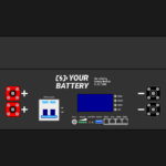
Defining Your Custom BMS Requirements
October 28, 2025